Automotive NVM: Grade 0 ambient and 175°C junction are not the same claim車規 NVM:Grade 0 環境溫度與 175°C 接面溫度不是同一項主張
This page uses the mission profile to pick the test gate. It does not issue a certification. AEC-Q100 Grade 0 is an ambient range (−40°C to +150°C Ta). Junction limits stay on the named datasheet.本頁依任務條件選擇測試關卡,不構成認證。AEC-Q100 Grade 0 是環境溫度(−40°C 至 +150°C Ta)。接面溫度以特定規格書為準。
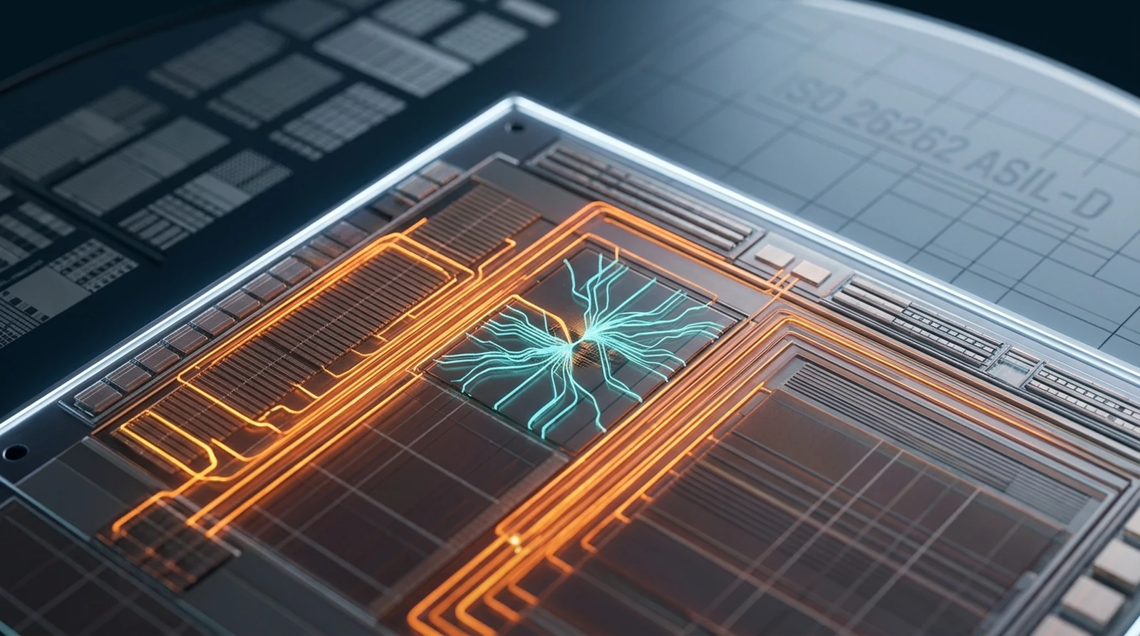
AI 生成概念背景 · 非裸晶照片AI-generated concept backdrop · not a die photograph
READING PATH閱讀路徑
Four gates before any ASIL sentence任何 ASIL 句子之前先走四關
Domain and mission profile first. Then Ta versus Tj. Then Q100-005 into HTOL / HTDR / ELFR. Stop at SEooC vocabulary and VERIFY.先定義領域與任務條件,再分 Ta 與 Tj,再走 Q100-005 到 HTOL/HTDR/ELFR。最後以 SEooC 術語收斂,數字維持待驗證。
Name the ECU domain and the time-at-temperature budget. That selects the grade conversation.先點 ECU 域與溫度時間預算。那才決定要談哪一等 Grade。
車規晶圓驗證需跨批次試驗與早期失效率篩選;本頁以任務載記與檢核清單語彙說明低缺陷目標,非宣稱已達 Zero-PPM 或 <0.001 PPM 認證。Automotive wafer qualification involves multi-lot audits and infant-mortality screening; this page uses mission-profile checklist vocabulary for low-defectivity targets — not a claim of Zero-PPM or <0.001 PPM certification.
GATE 01 · WAFER LOT AUDIT關卡 01 · 晶圓批次稽核
3-Lot 跨批次高溫壽命試驗 (HTOL)3-Lot Cross-Lot HTOL
跨越 3 個非連續晶圓生產批次,每批抽取 77 顆晶片在 175°C 接面溫度與 1.1× 標稱電壓下持續運行 1,000 小時。零單元擊穿退化,拒絕任何軟性位元翻轉。Across three non-consecutive wafer lots, 77 dice per lot run 1,000 hours at 175°C Tj and 1.1× nominal voltage. Zero cell breakdown; no soft-bit flips accepted.
通過 260°C 無鉛迴焊爐峰值衝擊,並依據 AEC-Q100-005 / JESD22-A103 執行高溫數據保持烘烤 (150°C 1,000 小時或 175°C 加速烘烤)。永久閘極介電質擊穿形成局域再結晶矽導電通道,高溫退火下幾無電荷漏失退化,確保在引擎周邊與逆變器長效運作 15 年以上。Survives 260°C Pb-free reflow peak, followed by AEC-Q100-005 / JESD22-A103 non-volatile data retention bake (150°C 1,000 hrs or equivalent 175°C accelerated bake). Permanent gate dielectric breakdown with localized recrystallized silicon percolation path exhibits named-condition ohmic stability (not absolute zero-drift certification) under thermal annealing, supporting architecture-class 15+ year automotive mission profiles.
LENS 02 · FLAGSHIP LAB 01觀點 02 · 主要實驗室 01
Arrhenius 熱加速教學模型Arrhenius Thermal Acceleration Teaching Model
調整溫度以計算相對 55°C 的熱加速因數。時間滑桿只移動標記,不計算保存年限。Adjust temperature to calculate acceleration relative to 55°C. The time slider moves a marker; it does not calculate retention life.
Ea = 0.84 eV 是未校準假設,非特定失效機制的量測常數。A/B 曲線未由 AF 推導,不對應產品家族、不證明性能優劣或認證。Ea = 0.84 eV is an uncalibrated assumption, not a measured failure-mechanism constant. Curves A/B are not derived from AF, represent no product family, and establish no performance ranking or qualification.NIST · Arrhenius
[ARRHENIUS THERMAL ACCELERATION MODEL][Arrhenius 熱加速模型] AF = exp[(Ea / kB) · (1/Tuse − 1/Tstress)]
(Tuse = 55°C (328.15 K) 教學基準teaching baseline, Ea = 0.84 eV 假設活化能 — 非量測常數assumed Ea — not a measured constant)
ISO 16750-2 / ISO 7637-2 規範ISO 16750-2 / ISO 7637-2 Spec
評估在 150°C~175°C 極限高溫結溫 (Tj) 下,交流發電機斷開引發的 ISO 16750-2 負載突降 (Pulse 5a / 5b) 與線束反衝瞬態脈衝灌入晶片電源軌時,主動式 MOSFET 電子保險絲與晶片內電荷泵 (Charge Pump) 升壓電路之動態箝位能力、介電質擊穿安全裕度與輸出漣波抑制比。Evaluates dynamic clamping performance, charge pump dielectric breakdown margin, and output ripple suppression under extreme 150°C~175°C junction temperature (Tj) when ISO 16750-2 load dump (Pulse 5a/5b) or inductive wiring kicks strike internal automotive NVM power rails.
⚠️ 示意模擬模型與技術邊界說明:⚠️ Schematic Model & Technical Boundary Notice:本工作台之 ISO 7637-2 / ISO 16750-2 拋負載 (Load Dump) 瞬態電壓與電荷泵鉗位響應為基於一階指數脈衝與簡化過電壓崩潰模型之數值示意,非實際車電晶片 EMC / ESD 實驗室認證數據。晶片在突波下的生存裕度取決於片上 TVS、高壓 BCD 製程耐壓窗與 PCB 外部濾波保護設計。The ISO 7637-2 / ISO 16750-2 load dump transient waveforms and charge pump clamping dynamics in this workbench are schematic numerical approximations based on first-order exponential pulses and simplified breakdown models, rather than lab-certified automotive EMC/ESD reports. Physical chip surge survival is governed by on-chip TVS clamps, high-voltage BCD design margins, and external PCB protection.
運算結溫 Tj:JUNCTION TJ:175 °C
目標箝位電壓門檻:TARGET CLAMP VOLTAGE:18 V
晶片端箝位峰值電壓PEAK CLAMPED V
—
晶圓輸入引腳實測Die supply pin
瞬態突波吸收峰值功耗PEAK SURGE POWER
—
保護電路瞬態負載Dynamic clamp load
電荷泵升壓漣波與壓降PUMP RIPPLE / DROOP
—
含 175°C 漏電懲罰Includes 175°C leakage
介電質擊穿安全裕度BREAKDOWN MARGIN
—
閘氧化層穿隧極限Gate oxide limit
車規合規性等級COMPLIANCE RATING
—
AEC-Q100 Grade 0 / ISOAEC-Q100 Grade 0 / ISO
車載電源完整性與高壓瞬態示波儀Automotive Power Integrity & Transient Scope
點擊或以鍵盤翻轉 64 資料位與 8 同位位元,觀察偶同位延伸漢明碼的症候 S 與整體同位 P。單錯可定位、雙錯可偵測;超過兩位可能誤校正或漏檢。本例不執行校正寫回、不模擬硬體陷阱,亦不證明 ASIL 或 FTTI。Toggle 64 data bits and 8 parity bits by pointer or keyboard to inspect syndrome S and overall parity P in an even-parity extended Hamming code. Single errors are located and double errors detected; more than two can miscorrect or go undetected. This example performs no correction write-back or hardware trap, and proves no ASIL or FTTI result.TI · (72, 64) ECC
等待模型載入Waiting for model
SYNDROME S · OVERALL PARITY P症候 S · 整體同位 P
—
DECODER INDICATION解碼器指示
—
MODEL BOUNDARY模型邊界
教學模型 · 非產品驗證Teaching model · not product validation
LENS 03C · FLAGSHIP LAB 04視角 03C · 旗艦實驗室 04
車用 ISO 26262 ASIL-D 瞬態軟錯誤 FIT 率、中子通量與 ECC 診斷覆蓋率試算器Automotive ISO 26262 ASIL-D Soft-Error FIT, Cosmic Neutron Flux & ECC Diagnostic Coverage Simulator
在電動車動力總成、BMS 電池管理與 L3/L4 自駕 ADAS 領域,宇宙射線大氣快中子(隨海拔高度指數增長)與封裝材料 Alpha 粒子是誘發隨機單粒子翻轉(SEU)的主要根源。本試算器依據第一性原理中子通量海拔衰減模型、單元臨界電荷與 SEC-DED / Chipkill 矩陣,計算硬體單點故障度量(SPFM ≥ 99%)、潛伏故障度量(LFM ≥ 90%)與週期性記憶體巡檢清洗(Scrubbing)對殘餘 FIT 率的抑制作業,嚴格驗證 ASIL-D 達成度。In EV traction inverters, BMS, and autonomous ADAS controllers, atmospheric fast neutrons (scaling exponentially with altitude) and packaging alpha emitters dominate transient soft-error rates (SER). Based on first-principles neutron altitude scaling, critical charge models, and SEC-DED/Chipkill syndrome matrices, this simulator evaluates Single Point Fault Metric (SPFM ≥ 99%), Latent Fault Metric (LFM ≥ 90%), and periodic scrubbing suppression on residual FIT, rigorously qualifying ISO 26262 ASIL-D targets.
⚠️ 示意模擬模型與技術邊界說明:⚠️ Schematic Model & Technical Boundary Notice:本試算器之單點故障度量 (SPFM)、潛伏故障度量 (LFM) 與宇宙射線中子翻轉 FIT 率為基於一階海拔通量縮放模型與典型 SEC-DED 症狀矩陣之工程示意試算,非經第三方認證機構 (TÜV SÜD 等) 簽署之產品級 FMEDA 安全報告。車規功能安全設計需依循完整 ISO 26262 流程管理與硬體失效率分配。The Single Point Fault Metric (SPFM), Latent Fault Metric (LFM), and neutron soft-error FIT rates in this simulator are engineering schematic calculations based on first-order altitude flux scaling and typical SEC-DED syndrome matrices, not product-level FMEDA reports certified by third-party bodies (e.g. TÜV SÜD). Automotive functional safety must comply with full ISO 26262 lifecycle processes and hardware failure apportionment.
行車海拔高度:DRIVING ALTITUDE:1500 m
記憶體容量:ARRAY CAPACITY:16 Mb
巡檢清洗週期:SCRUB INTERVAL:60 s
原始中子軟錯誤率RAW SER FIT
--
殘餘單點故障率 (SPF)RESIDUAL FIT
--
單點故障度量 (SPFM)SPFM METRIC
--
潛伏故障度量 (LFM)LFM METRIC
--
ISO 26262 ASIL Functional Safety Analyzer
Loading ISO 26262 ASIL-D safety calculations...
ASIL-D TARGET MET
車規高壓物理模型HIGH-VOLTAGE AUTOMOTIVE MODEL
800V EV 電池管理 (BMS) 共模瞬態 (CMTI) 與快照日誌模擬器800V EV BMS CMTI Isolation & Crash Freeze-Frame Journal Simulator
⚠️ 示意模擬模型與技術邊界說明:本模型基於 ISO 26262 ASIL-D 功能安全準則與 SiC 逆變器高頻開關 (dV/dt) 集中參數計算,模擬 BMS 斷電快照寫入裕度,非特定車載電池包之實車崩潰破壞性測試。⚠️ Illustrative Simulation Model & Technical Boundary Note: Grounded in ISO 26262 ASIL-D functional safety criteria and SiC inverter dV/dt displacement current equations; illustrative only.
在 800V 電動車動力系統中,SiC MOSFET 逆變器產生極高共模瞬態噪聲 (CMTI > 150 kV/µs),透過隔離屏障產生位移電流衝擊電芯監控 AFE 晶片。當發生熱失控或高壓斷開事故時,BMS 晶片內建 NVM 必須在毫秒級掉電保溫窗 (Power-Hold Window < 2ms) 內完成全電芯電壓與溫度黑盒子快照寫入。In 800V EV powertrains, SiC MOSFET switching induces severe Common-Mode Transient Noise (CMTI > 150 kV/µs), driving displacement currents across galvanic isolation into battery cell monitoring AFEs. During thermal runaway, embedded NVM must complete critical freeze-frame telemetry within a 2ms power-hold window.
隔離位移電流 (I_disp)Displacement Current225.0 mA
CMTI 抗擾安全裕度CMTI Safety Margin1.33× Margin
緊急快照寫入耗時Freeze-Frame Latency1.20 ms
ASIL-D 滿分適配:在 800V SiC 高頻開關下具備充裕 CMTI 裕度,且於 2ms 斷電緩衝期內完成全電芯黑盒子快照寫入。ASIL-D Fully Compliant: Robust CMTI margin under 800V SiC transients; completes full freeze-frame write within 2ms crash buffer.
LENS 03D · FLAGSHIP LAB 05視角 03D · 旗艦實驗室 05
車規自駕 HPC / AI 加速器 HBM4 極限任務剖面、動態 sPPR / hPPR 巡檢清洗與 FIT 率退化模擬器Automotive ASIL-D HBM4 Extreme Mission Profile, Dynamic sPPR / hPPR Scrubbing & FIT Degradation Simulator
在 L4/L5 無人自駕計程車與重型自駕商用車中,HBM4 晶粒堆疊面臨 115°C~125°C 高溫、高原高海拔大氣快中子通量與強烈熱循環應力。本模擬器結合 Coffin-Manson 焊點熱疲勞模型與 Arrhenius 軟錯誤熱加速,模擬週期性記憶體巡檢清洗(Scrubbing)與 Base Die 內建之動態 sPPR 暫存器熱修復、永久 0-Mask AntiFuse OTP hPPR 壞列硬體重映射,評估達成 ISO 26262 ASIL-D 設計度量目標(SPFM ≥ 99%, 單晶粒殘留 FIT < 10)之可行邊界。In L4/L5 Robo-Taxis and heavy commercial autonomous trucks, HBM4 3D stacks face 115°C–125°C junction temperatures, high-altitude neutron flux, and severe thermal fatigue. Combining Coffin-Manson solder fatigue with Arrhenius soft-error acceleration, this simulator models periodic scrubbing, Base Die dynamic sPPR cache, and permanent 0-Mask AntiFuse OTP hPPR row remapping, evaluating feasibility boundaries toward ISO 26262 ASIL-D design targets (SPFM ≥ 99%, residual FIT < 10).
⚠️ 示意模擬模型與技術邊界說明:⚠️ Schematic Model & Technical Boundary Notice:本工作台之失效率 (FIT)、SPFM 單點故障度量與 hPPR 消耗估算為基於 JEDEC JESD89A 大氣中子數據、Arrhenius 熱活化能與 Coffin-Manson 焊點熱疲勞之數值示意模型,非第三方實體驗證之 ASIL-D 產品認證報告。ISO 26262 系統級功能安全需經完整 FMEDA 分析與產品安全生命週期管理;實際晶片失效率受封裝基板底部填膠 (Underfill) 應力及冷卻散熱設計影響。The FIT failure rates, SPFM metrics, and hPPR usage estimates in this workbench are numerical schematic models based on JEDEC JESD89A atmospheric neutron data, Arrhenius thermal activation, and Coffin-Manson fatigue models, rather than third-party ASIL-D certified product test reports. ISO 26262 functional safety requires rigorous FMEDA analysis and lifecycle management; physical chip reliability is governed by substrate underfill integrity and active thermal management.
Base Die 接面溫度 (Tj):JUNCTION TEMP (Tj):115 °C
巡檢清洗週期:SCRUB PERIOD:1.00 s
HBM4 堆疊容量:STACK DENSITY:64 GB
原始累積失效率RAW ACCUM FIT
--
清洗後殘餘失效率RESIDUAL FIT
--
單點度量 SPFMSPFM METRIC
--
AntiFuse hPPR 消耗hPPR USAGE
--
ISO 26262 ASIL-D & AEC-Q100 車規溫度參照分析器ISO 26262 ASIL-D & AEC-Q100 Automotive Temperature Reference Analyzer
基於載子凍結、不完全游離、總游離劑量 (TID) 氧化層電洞陷阱漂移與重離子 SEU 韋伯 (Weibull) 截面積模型,評估從 4.2K 液氦超導量子控制到 500 krad 深空木星強輻射下 eNVM 物理可行性。Phenomenological modeling of carrier freeze-out, incomplete ionization, Total Ionizing Dose (TID) hole trap accumulation, and heavy-ion SEU Weibull cross-section across 4.2K cryo-CMOS and 500 krad Jovian radiation belts.
⚠️ 示意模擬模型與技術邊界說明:⚠️ Schematic Model & Technical Boundary Notice:本工作台之 4.2K 載子凍結、次閾值擺幅與總電離劑量 (TID) 閾值漂移推估為基於簡化低溫物理與 Weibull 重離子截面積之數值模型,非單一 IP 官方太空或極低溫認證報告。深空 Class-S 或量子計算周邊之實際可靠度需依 MIL-STD-883 方法 1019 實施鈷-60 (Co-60) 射源與迴旋加速器實體重離子測試。The 4.2K carrier freeze-out, subthreshold swing, and TID shift projections in this workbench are schematic numerical models based on simplified cryogenic physics and Weibull cross-sections, rather than formal spaceflight qualifications. Real-world mission assurance requires empirical Cobalt-60 and cyclotron heavy-ion irradiation testing per MIL-STD-883 Method 1019.
⚠️ 示意模擬模型與技術邊界說明:⚠️ Illustrative Model & Boundary Notice: 本模擬器採用 Arrhenius 熱活化加速與去飽和保護 (DESAT) 之簡化工程模型,用以示意高溫下電荷洩漏、磁穩定性與微絲擴散之相對趨勢。第三代半導體功率開關裸晶高溫合封環境下,浮閘 eFlash 因熱發射效應面臨電荷洩漏加速,通常配置於溫度較低之微控制器晶粒;AntiFuse 微絲介質耐溫性良好,但仍需考量高壓編程脈衝為單次不可逆寫入之系統架構邊界。所列評級為工程適配分類,非車規官方認證。This simulator uses simplified Arrhenius thermal activation and DESAT timing models to illustrate trends in charge leakage, magnetic stability, and filament diffusion. In high-Tj power co-packaging environments, floating-gate eFlash experiences accelerated thermionic emission and is typically located on cooler MCU dies; AntiFuse silicide filaments offer robust temperature tolerance, though system designs must account for its irreversible OTP nature. Tiers represent engineering classifications rather than official certifications.
ADC 增益偏差、帶隙基準電壓、LiDAR 光學陣列校準。僅限出廠封裝與受控車廠 OTA 維護時進行有限次數單向補丁。ADC gain offsets, bandgap voltages, and LiDAR calibration arrays. Bounded to factory testing and authorized OEM maintenance.
ISO 26262 ASIL-D vocab (SEooC)ISO 26262 ASIL-D 術語(SEooC)
CONTRACT 02 · Trim契約 02 · 微調
AntiFuse Counter反熔絲計數器
示意值 · 需 FMEDAIllustrative · FMEDA req.
示意值 · 需 FMEDAIllustrative · FMEDA req.
示意 · 非量測Example · not measured
ISO 26262 ASIL-D vocab (SEooC)ISO 26262 ASIL-D 術語(SEooC)
CONTRACT 03 · Recovery契約 03 · 復原
SECDED OTP MacroSECDED OTP 巨集
示意值 · 需 FMEDAIllustrative · FMEDA req.
示意值 · 需 FMEDAIllustrative · FMEDA req.
示意 · 非量測Example · not measured
ISO 26262 ASIL-D vocab (SEooC)ISO 26262 ASIL-D 術語(SEooC)
Industry Baseline · eFlash產業基準 · eFlash
Floating-Gate浮動閘極
教學對照 · 非 FMEDATeaching contrast · not FMEDA
教學對照 · 非 FMEDATeaching contrast · not FMEDA
教學對照Teaching contrast
需依賴雙單元或外部進階 ECC 機制以支援系統級 ASIL-D 目標Requires dual-cell or external advanced ECC to support item-level ASIL-D target
SEooC 假定使用條件 (AoU): 上表 SPFM/LFM/PMHF 僅為教學示意,須以具名 FMEDA 與產品整合關閉。SEooC 流程可使用 ISO 26262 ASIL 詞彙(非 READY 認證);IEC 61508 SC3 為跨標準教學對照,本頁架構不宣稱具備。系統級 ASIL 達成須 Tier-1/OEM 整合外部安全機制(看門狗、電源監控、SECDED 雙位元陷阱)。潛伏故障度量 LFM 依 Tscrub ≤ Tlatent_budget 等 AoU 而定 — 不得由本頁表格直接推出認證。SEooC Assumptions of Use (AoU): SPFM/LFM/PMHF in the table are teaching illustrations only — close with named FMEDA and product integration. SEooC may use ISO 26262 ASIL vocabulary (not READY certification). IEC 61508 SC3 is a cross-standard teaching reference — this page does not claim that capability by architecture alone. Item-level ASIL requires Tier-1/OEM external safety mechanisms. Latent-fault metrics depend on AoU such as Tscrub ≤ Tlatent_budget — do not infer certification from this page alone.
⚠️ 示意模擬模型與技術邊界說明:⚠️ Illustrative Model & Technical Boundary Notice: 本試算器採用電容儲能恆等式 E = 0.5·C·(V_start² - V_uvlo²) 與簡化寫入功耗積分,用以示意斷電瞬間持電電容容值需求與黑盒子快照寫入時長。實際車規 ECU / PMIC 之應急寫入能力取決於電源軌動態負載、電容等效串聯電阻 (ESR)、高低溫老化容值降額 (Derating) 及軟體非揮發快照提交延遲。This simulator employs the capacitor energy equation E = 0.5·C·(V_start² - V_uvlo²) and simplified write power integration to illustrate hold-up capacitance requirements and crash-dump durations. Actual ECU/PMIC emergency logging relies on dynamic rail loading, capacitor equivalent series resistance (ESR), lifetime thermal derating, and firmware persistence commit latency.
[上游代工][Foundry]0.18µm 與 65nm BCD 平台原生支援,零額外光罩 (0 Mask Adders);依 Tower 一次來源為 CHE 寫入/BBT 抹除(非 FN/FN)。Native 0.18µm and 65nm BCD platforms with 0 mask adders; per Tower primary sources, CHE program / BBT erase (not FN/FN).
[車規耐溫][Automotive Grade]官方文件提及 Grade 0 保持敘事;環境溫度 Ta(-40~+150°C)與接面 Tj 試驗條件須分開。製造流程無額外熱預算敘述需對應具名平台,不得等同全系統認證。Vendor briefs cite Grade 0 retention narratives; separate ambient Ta (-40 to +150°C) from junction Tj test conditions. Zero extra thermal-budget claims apply to named platforms, not blanket system certification.
[下游系統][Downstream Systems]車載電池管理系統 (BMS) 電池單元阻抗黑盒子查表、48V 伺服器/車載 VRM 數位電源控制、智慧高壓閘極驅動 IC。Automotive BMS cell impedance lookup tables (LUT), 48V server/automotive VRM digital power control, and intelligent high-voltage gate drivers.
[上游代工][Foundry]TSMC / UMC 40nm 至 5nm 車規標準邏輯 CMOS 製程,0 額外光罩,相容嚴苛晶圓簽核門禁。Standard automotive logic CMOS (40nm down to 5nm) at TSMC and UMC; 0 mask adders with standard signoff compatibility.
[微縮斷崖挑戰][Scaling Cliff Challenge]7nm/5nm/3nm 先進 FinFET/GAA 邏輯節點由於額外光罩成本暴增 30%+ 與高溫退火破壞電晶體,無法內建傳統 eFlash。Advanced FinFET/GAA nodes (7nm/5nm/3nm) cannot integrate legacy eFlash due to 30%+ mask adder cost escalation and thermal degradation of logic transistors.
[異質整合解法][Heterogeneous Solution]採用專用車規 Grade 0 (45nm/28nm) NOR Flash 之 KGD (Known Good Die) 晶圓裸晶、WLCSP / USON 超小型封裝,進行 2.5D/3D SiP (System-in-Package) 緊密堆疊。Leverages automotive Grade 0 (45nm/28nm) NOR Flash Known Good Die (KGD) and ultra-compact WLCSP/USON packages for 2.5D/3D System-in-Package (SiP) stacking.
[下游系統][Downstream Systems]透過 Octal SPI / xSPI 介面提供高達 400MB/s 頻寬與晶片外就地執行 (XiP),於自動駕駛 ADAS 域控制器與智慧座艙達成 50ms 內極速冷啟動 (Instant-On Boot)。Delivers up to 400MB/s bandwidth via Octal SPI / xSPI with Execute-in-Place (XiP), achieving sub-50ms instant-on boot in ADAS domain controllers and smart cockpits.
[上游代工][Foundry]ST 公開資料說明 GST 相變材料整合於 28 nm 與 18 nm FD-SOI 平台;Stellar P3E 簡報具體列出 28 nm FD-SOI PCM。相關材料與平台揭露不等於所有料號的製程光罩數或完整抗輻射保證。ST describes GST phase-change material on 28 nm and 18 nm FD-SOI platforms; the Stellar P3E presentation specifically lists 28 nm FD-SOI PCM. Material and platform disclosures do not establish mask counts or complete radiation immunity for every part.
[相變物理特徵][PCM Physics]PCM 透過電脈衝加熱切換非晶態(高阻)與晶態(低阻)。ST 的技術頁宣稱可在最高 165°C 操作;操作溫度不等於資料保持測試溫度,寫入速度、保持年限與耐寫條件仍須核對具名料號。PCM uses electrical heating to switch between amorphous high-resistance and crystalline low-resistance states. ST’s technology page claims operation up to 165°C; operating temperature does not establish retention test temperature. Write speed, retention lifetime and endurance conditions require named-part documentation.
[下游系統][Downstream Systems]Stellar P3E 公開簡報介紹 xMemory 與 OTA 功能,作為車用軟體更新的架構能力。更新時機、執行隔離、切換與復原須依 ECU 和整車安全策略設計;此揭露不保證所有車輛可在行駛中零停機升級。The Stellar P3E presentation describes xMemory and OTA as architectural capabilities for automotive software updates. Update timing, execution isolation, switchover and recovery depend on ECU and vehicle safety strategies; the disclosure does not guarantee zero-downtime updates while driving for every vehicle.
[產品記憶體][Product Memory]NXP S32Z2 官方規格為 16nm 處理器,最多整合 64 MB Flash,列為 AEC-Q100 Grade 1 元件;此容量與資格屬 S32Z2,不能改標為 64 MB eMRAM。NXP specifies S32Z2 as a 16nm processor with up to 64 MB integrated Flash and AEC-Q100 Grade 1 qualification. These specifications belong to S32Z2 and do not describe 64 MB of eMRAM.
[核心與更新][Cores & Updates]官方列出 Cortex-R52 核心最高 1 GHz,以及處理器無停機的 OTA 能力。核心時脈不是 NVM 存取延遲;整車服務連續性與更新切換仍須系統設計及驗證。NXP lists Cortex-R52 cores up to 1 GHz and OTA capability with zero processor downtime. Core frequency does not specify NVM access latency; vehicle-service continuity and update transitions still require system design and validation.
[eMRAM 路線與系統應用][eMRAM Roadmap & Applications]NXP/TSMC 於 2023 年宣布共同開發 16nm FinFET eMRAM,面向下一代 S32 區域處理器與通用車用 MCU,當時規劃 2025 年初提供產品樣品。該公告未將其指定為 S32Z/E,也不能作為目前量產或特定料號資格證明。The 2023 NXP/TSMC announcement described joint 16nm FinFET eMRAM development for next-generation S32 zonal processors and automotive MCUs, with product samples then planned for early 2025. It did not identify S32Z/E or establish current production or part-specific qualification.